— #
math: true #
DESIGN AND IMPLEMENTATION #
APPROACH #
The main approach used to meet the objectives of this project was the systems engineering approach. This section is divided into sub-sections.
Input filter #
The first step to the solution is to rectify the input voltage and current from the mains supply. This will require a full bridge rectifier with an output capacitor. Full bridge rectifiers can easily be purchased off the shelf, but for this project it will be designed from first principles. Diodes that provide the least voltage drop when conducting will be used to minimize power loss in this stage of the overall system. The input filter is also the first step to prevent EMI from the main’s supply input voltage and current.
DC-DC converter topology #
There are several ways to reach the desired voltage output, one way is to step up the voltage to 230V DC and then invert it. This approach however will need components that can handle higher voltages and currents. The control of these power electronic circuits could prove to be troublesome because of the high voltages. The other approach is to step down the input voltage to 17V DC and then invert it into AC, this then is fed into a transformer (20:1 step up transformer to create the final 230Vac output). This approach is more practical and safer to build because of the lower voltages but adds bulk to the overall system. The transformer also increases the harmonics. The approach with the lower voltages was chosen.

Approach using a step up converter

Approach using a buck converter with a transformer
According to the literature study, there are numerous step down DC-DC converters, the final choice was either between the conventional buck converter and the flyback converter. The buck converter was chosen since it can meet up with the power requirements and simplifies the design process since an inductor is needed rather than a flyback transformer.
The choice of the switching frequency is important, Most of the losses in a SMPS system are contributed by the switching losses, this means the switching frequency chosen should be fast to minimize losses and at the same time not be too fast to produce unnecessary EMI (normally between 70kHz and 300kHz) according to [11]. The switching frequency is also based on the inductor material that is used.
According to the literature study, the power MOSFET is better for high frequency and low power application so therefore it was chosen as opposed to the IGBT. The MOSFET switch for the buck converter will be chosen based on the maximum stress voltage maximum peak input current, total power losses, maximum allowed operating temperature, and current driver capability of the driver. Besides maximum voltage rating, and maximum current rating, the others three important parameters of a MOSFET are Rds1(on), gate threshold voltage, and gate capacitance.
The buck converter will be modelled by differential equations and will initially be designed as an ideal circuit. From this model, non-ideal components will be added and the final state space and laplace transforms will determined to design the control circuit. The ideal state space equations will be used to size the switches and inductor with a 20% tolerance.
The buck converter’s inductor itself will be designed with the selected switching frequency being the core of the design process. The most important aspect of a buck converter is the inductor which can also be considered. The design of the inductor has to take into account various other factors such as:
-
Operating temperatures
-
Flux density
-
Core saturation
-
Magnetising flux
-
Leakage flux
-
Winding loss and currents
Based on these factors the core will be selected with the final windings.
The final buck converter circuit has to be able to handle the heat dissipation and spikes of the switches which means a thermal design and snubber circuits are needed.
Inverter #
Part of the requirements was to have a smooth sine wave output so the only choice was between the half bridge and full bridge converter. Full bridge converter was chosen since its switches require half the ratings compared to a half bridge inverter and the output of the buck converter needs only to be 17V (as opposed to 34V if it was a half bridge converter).
The next important criteria is to select $M_{a\ }$and $M_{f}$ and the switching scheme. Theoretically the value of $M_{a\ }$will be selected within the range of 0.8-0.9 and the $M_{f}$ will be set to a value that will minimize harmonics. Based on the literature study for the switching schemes, the digital switching scheme was chosen since it is less cumbersome to implement as opposed to the more analog based (unipolar and bipolar) schemes. This also means that $M_{a\ }$and $M_{f}$ can be ignored.
The full bridge inverter will be modelled by differential equations and will initially be designed as an ideal circuit. From this model, non-ideal components will be added and the final state space and laplace transforms will determined to design the control circuit.
For similar reasons with the selection of the switch type in the buck converter, the power MOSFET will once again be selected as opposed to the IGBT. The MOSFET switch for the full bridge inverter will be chosen based on the maximum stress voltage maximum peak input current and total power loss.
Final full bridge inverter circuit has to be able to handle the heat dissipation and spikes of the switches which means a thermal design and snubber circuits are needed.
DETAILED DESIGN AND IMPLEMENTATION #
Overall design #
The wind synchronization project is comprised of sub-systems and each one has its own specifications and requirements. Shown below is a flow diagram of the overall system and a network diagram of subsystems that make up the project:
Network diagram of proposed system
The project consists of two main systems and two systems. The two main systems are the AC-DC converter and the DC-AC inverter. The two subsystems are the power supply and the output filter. The power supply is responsible for powering the microcontrollers and gate drivers. The output filter ensures that the output of the inverter will be a smooth sinusoidal signal. This section will first cover the two main systems and then the subsystems will be discussed.
Input Filter design #
Since the input to the system is an AC signal (20-60Vac, 0-300Hz), the first step is to rectify it with a full bridge rectifier2 and a capacitor. The selection and sizing of the capacitor will determine the voltage ripple of the output. Shown below is the circuit schematic of the input stage of the system:
12.](media/image4.png){alt=“C:\Users\PVT\Desktop\Wind integration\Simulations\Full.png” width=“3.1927766841644796in” height=“1.5748698600174977in”}
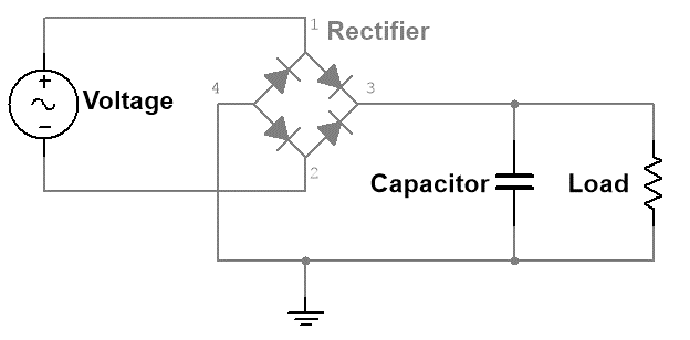
Circuit diagram of the input stage of the system
The following equation was used to determine the capacitor size,
$$ C_{filter} = \frac{0.045 P_{load}}{\eta (V_{in, min, pk})^2} $$ (1) #
Where $C_{filter}$is the value of the input capacitor (Farads, F); $P_{load}$ is the load of the circuit (Watts, W); $\eta$ is the efficiency of the converter and is assumed to be 60% and $V_{in,\ min.\ pk}$ is the minimum input voltage (Volts, V). The respective values were substituted in equation (1).
$$C_{in} = \frac{0,045 \times 100}{0.6 \times {(\sqrt{2} \times 20)}^{2}} = 120uF$$ (2)
A safety factor of 2 was used to rate the voltage tolerance of the input capacitor. The maximum is assumed to be 100Vdc which translates to a 200Vdc capacitor with a value of 120uF.
Buck Converter design #
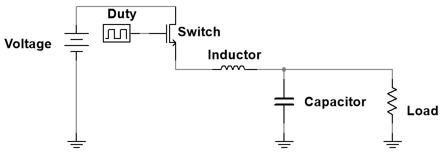
The input voltage range is between 20 – 60 Vac (processed into a DC voltage by the input filter, 3.1.1), which translates to approximately 25-85Vdc. A buck converter will be used to step down the voltage to 17V. The ideal circuit schematic of the buck converter is shown below:
![[]{#_Ref397276600 .anchor}Figure
13.](/focus/projects/inverter-design-from-first-principles/media/image5.png)
Circuit diagram of an ideal buck converter.
The important circuit parameters of the circuit are the inductor and capacitor. These two components determine the output current and voltage. There are two distinct operation modes for this converter, one is when the “switch” is “on” and the second is when the “switch” is “off”. Shown below is effectively how the circuit behaves when the “switch” is “on”:
How the buck converter circuit effectively behaves like when the "Switch" is "on".
While the “switch” is conducting, the diode in Figure 13 is bypassed. When a KVL loop is applied to the above circuit, one gets the following governing equation:
$$V_{dc} = V_{ce} + i_{L}.R_{L} + V_{out} + V_{L}$$ (3)
Where $V_{dc}$ is the input voltage (Volts, V); $V_{ce}$ is the voltage of the “switch” when conducting (Volts, V); $i_{L}$ is the current of the inductor (Amperes, A); $R_{L}$ is the effective resistance of the inductor and is measured (Ohms, Ω) and is assumed to be negligible; $V_{out}$ is the output voltage with respect to the load (Volts, V) and $V_{L}$ is the voltage of the inductor (Volts, V).
When a KCL loop is applied, one gets the following governing equations:
$$i_{L} = i_{c} + i_{out}$$ (4)
$$i_{L} = i_{sw}$$ (5)
Where $i_{c}$ is the current of the capacitor (Amperes, A); $i_{out}$ is the output current as measured from the load (Amperes, A) and $i_{sw}$ is the current of the “switch” (Amperes, A).
When the “switch” is “off”, the current dynamics of the system changes. Shown below is effectively how the circuit behaves when the “switch” is “off”:
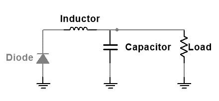
How the buck converter circuit effectively behaves like when the "Switch" is "off".
During this phase, the input voltage and “switch” can be ignored since the power now is being transferred from the inductor and capacitor into the load. When a KVL loop is applied to the above circuit, one gets the following governing equation:
$$V_{FWD} = i_{L}.R_{L} + V_{out} + V_{L}$$ (6)
Where $V_{FWD}$ is the voltage of the diode when it is forward biased (Volts, V) and is approximately 1,2V according to the specific diode used3.
When a KCL loop is applied, one gets the following governing equations:
$$i_{L} = i_{D}$$ (7)
Where $i_{D}$ is the current of the “free wheeling” diode (Amperes, A).
The voltage across the inductor is zero over one cycle. During “Ton”: $i_{L}.R_{L} = V_{DC} + V_{CE} - V_{out} = V_{L}$ and during “Ton”: $i_{L}.R_{L} = V_{FWD} - V_{out}$. Substituting the equations with each other yields the following equation:
$$\delta = \frac{V_{FWD} + i_{L}.R_{L} + V_{out}}{V_{dc} + V_{FWD} - V_{CE}}$$ (8)
Where $\delta$ is the duty ratio.
Based on the above duty ratio equation, the duty ration range was determined with a 10% tolerance for an input voltage range of 20-90Vdc. $V_{CE}$is assumed to be 1,5V when it is turned on.
$$\delta_{\max} = \frac{1,2 + (5,88 \times 0) + 17}{20 + 1,2 - 1,5} = 0,925$$ (9)
$$\delta_{\min} = \frac{1,2 + (5,88 \times 0) + 17}{90 + 1,2 - 1,5} = 0,205$$ (10)
Therefore the duty ratio range is 0,205 - 0,925.
Current through an inductor ($L$) can be used to find the voltage across an inductor ($V_{L}$), with the use of the following fundamental equation:
$$V_{L} = L.\frac{di}{dt}$$ (11)
$$\therefore\frac{di}{dt} = \frac{V_{L}}{L}$$ (12) #
Over one switching cycle, the average voltage of the inductor has to be zero to avoid the saturation of the inductor.
$${\Delta i}{L,pk - pk} = \frac{\left( V{DC} - V_{CE} - i_{L}.R_{L} - V_{out} \right).\delta.T_{SW}}{L}$$ (13)
$$L_{\min} = \frac{\left( V_{DC} - V_{CE} - i_{L}.R_{L} - V_{out} \right).\delta.T_{SW}}{{\Delta i}_{L,pk - pk}}$$ (14)
Where $\frac{di}{dt}$ is the change in current of the inductor (Amperes per second, $A.s^{- 1}$); $V_{L}$ is the voltage of the inductor (Volts, V); $L$ is the inductance of the inductor (Henry, H) is and ${\Delta i}_{L,pk - pk}$ is the peak to peak current of the inductor (Amperes, A).
To determine ${\Delta i}_{L,pk - pk}$, the output current of the buck converter needs to be known and can be found out by using the following formulae.
$$P_{out} = V_{out}.I_{out}$$ (15)
$$I_{L,ave} = I_{out}$$ (16)
Where $P_{out}$is the output power of the buck converter which is selected to be 100W; $V_{out}$ is the output voltage which is 17Vdc; $I_{L,ave}$ and $I_{out}$are the average inductor current and the output current respectively (Amperes, A).
Based on the above formulas, the $I_{L,ave}$ was calculated to be 5,88A
Therefore the minimum inductance needed is found with the assumption that the peak to peak inductor current is 25%:
$$L_{\min} = \frac{\left( 90 - 1,5 - (5,88 \times 0) - 17 \right) \times 0,205}{(0,25 \times 5,88) \times 25000} = 830uH$$ []{#_Ref402694419 .anchor}(17)
During switching the current through the inductor is split in half:
$0 < t <$ $\delta.T_{SW}$ is the switch current ($i_{SW}$).
$\delta.T_{SW} < t <$ $T_{SW}$ is the diode current ($i_{D}$).
$$I_{L,RMS} = I_{L,avg}\sqrt{1 + \frac{1}{\delta}\left( \frac{\frac{{\Delta i}{L,pk - pk}}{2}}{I{L,avg}} \right)^{2}}$$ (18)
Therefore the RMS current of the inductor is:
$$I_{L,RMS} = 5,88\sqrt{1 + \frac{1}{0,205}\left( \frac{\frac{0,1 \times 5,88}{2}}{5,88} \right)^{2}} = 5,916A$$ (19)
By removing the DC offset of the inductor current, one can get the capacitor current since the capacitor current processes the ripple content of the current. The ripple voltage is set to be 10%.
Output capacitor #
The selection of the output capacitor depends on the type of converter, ripple tolerance and operating frequency. A well-chosen capacitor will produce a smooth output with negligible losses. The performance of a capacitor in terms of the ripple is based on the ESR of the capacitor. The ESR has a direct influence on the output ripple and since it is acts as a passive dissipative element, it generates heat which reduces the life span of a capacitor.
To find out the value of the capacitor needed, one has to have a look at the current waveform of the capacitor. The current oscillates around the zero point with a peak value of half the ripple. If one integrates the area of one time period of this waveform, the $C_{out}$ value can be calculated.
$$V_{out} = \frac{1}{C_{out}}\int_{t_{1}}^{t_{2}}{\ i}.dt$$ *(20**)*
The average current between the interval of $t_{2}$ and $t_{1}$ is $\frac{{\mathrm{\Delta}I}_{out}}{4}$. Based on this value, when one integrates the above integral the following equation will yield the following:
----------------------------------------------------------------------------------------------------------------
$$
V_{out} = \frac{I_{out} T}{4 C_{out}} = \frac{(\Delta I_{out}) T}{8 C_{out}}
$$
*(21)*
----------------------------------------------------------------------------------------------------------------
Where T is the time interval between $t_{2}$ and $t_{1}$. Rearranging the above expression to make the output capacitor the subject of the formula.
-------------------------------------------------------------------------------------------
$$
C_{out} = \frac{\Delta I_{out}}{8 f \Delta V_{out}}
$$
*(22)*
-------------------------------------------------------------------------------------------
Where $f$is the operating frequency ($\frac{1}{T}$) (Selected to be 25kHz). It was specified that the output ripple of both the voltage and current should be 10%. A safety margin will be used to ensure even better performance by assigning a 0.05% voltage ripple for the output voltage and a 10% ripple for the current, this will ensure a larger capacitor value and therefore a smoother output.
---------------------------------------------------------------------------
$$
C_{out} = \frac{0.1 I_{out}}{8 f (0.005 V_{out})}
$$
*(23)*
---------------------------------------------------------------------------
Once the values get substituted in the above equation;
$$ C_{out} = \frac{0.1 \times 5.88}{8 \times 25 \times 10^{3} \times (0.005 \times 17)} = 345uF $$ (24) #
As mentioned earlier that the ESR of a capacitor determines the ripple, therefore the maximum ESR value to produce the above voltage and current ripple is;
$${ESR}{\max} = \frac{{\mathrm{\Delta}V}{out}}{{\mathrm{\Delta}I}_{out}} = \frac{0,095}{1} = 0,095\Omega$$ (25)
If the above ESR value cannot be obtained from one capacitors then a possible solution is to connect the capacitors in parallel, since the ESR acts just like normal resistors when connected in parallel.
Shown below are simulation results for the ideal buck converter with a 90V and 20V DC input:
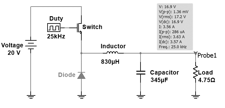
Ideal buck converter circuit with 90V input with a duty ratio of 0.85.
![[]{#_Ref400813774 .anchor}Figure
17.](/focus/projects/inverter-design-from-first-principles/media/image9.png)
Output voltage of buck converter with 20V input and duty ratio of 0.85.
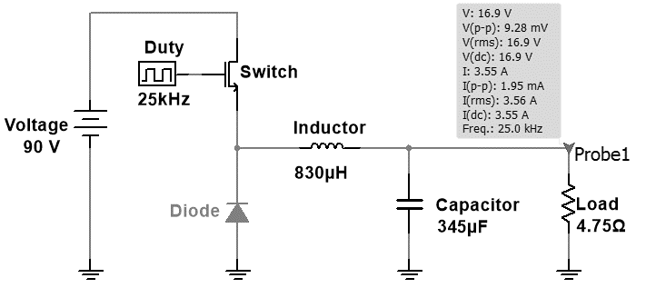
Ideal buck converter circuit with 90V input with a duty ration of 0.18
![[]{#_Ref400814968 .anchor}Figure
19.](/focus/projects/inverter-design-from-first-principles/media/image11.png)
Output voltage and current of buck converter with 90V input with a duty ratio of 0.18.
Comparing the above simulation (Figure 17 and Figure 19) results shows that the output voltage and current are identical. The only difference with the simulated circuit is the duty ratios.
Inductor #
The design of the inductor is determined by the following design inputs; the peak, average and RMS current the inductor has to process, the switching frequency, ambient and inductor surface temperatures and the inductance [12].
Analyzing the waveform of the inductor current determines if the inductor needed is needed for a DC or AC application. If the polarity is never negative then a DC inductor is needed and operates in one quadrant. Hence the frequency of the inductor is not an issue since the hysteresis is negligible. There are various materials that can be used to make up the core of this inductor like METGLAS, steel or ferrites.
Ferrite was chosen since it suited the particular application based on frequency. The only available core type available was the N27 ferrite with a maximum $B_{c}$ of 350mT according to the B-H curve in the datasheet. One should choose a $B_{c}$ near the curve of the “knee”. The ripple percentage of the $B_{c}$ should be the same as the ${\Delta i}_{L,pk - pk}$ to avoid saturation.
$$J_{RMS} = \sqrt{\frac{P_{c,sp}}{k_{cu}.p_{cu}.\left( \frac{R_{AC}}{R_{DC}} \right)}}$$ (26)
Where $J_{RMS}$ is the current density of the inductor winding (Amperes per area squared, $\frac{A}{{mm}^{2}}$); $P_{c,sp}$ is the power capacity as according to the core material’s datasheet (Watts per volume, $\frac{kW}{m^{3}}$); $p_{cu}$ is the conductivity of copper which is $2.2 \times 10^{- 8}$Ʊ; $\frac{R_{AC}}{R_{DC}}$ is the ratio of the AC and DC resistance of the wire, which is a 1 for a DC system; $k_{cu}$ is the copper fill factor which is assumed to be 0.45 in a DC system since stranded wire is not needed.
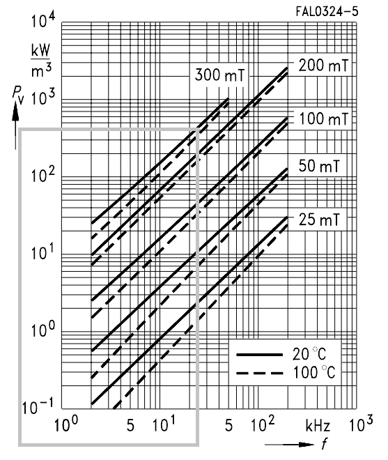
Relative core loss versus frequency with a selected frequency of 25kHz at 300mT
Based on the above graph4, the frequency was selected for 25kHz with a flux density of 300mT.
Therefore;
$$J_{RMS} = \sqrt{\frac{370}{0,45 \times 2.2 \times 10^{- 8} \times 1}} = 5,9 \times 10^{6\ }A.m^{- 2}$$ (27)
The window product is shown below:
$$A_{w}.A_{c} = A_{p} = \frac{L.I_{L,pk}.I_{L,RMS}}{k_{cu}.B_{core}.J_{RMS}}$$ (28)
Where $L$ is the inductance of the inductor calculated previously with equation (17) for the buck converter (H, henry); $I_{L,pk}$ and $I_{L,RMS}$ are the peak and RMS currents of the inductor as calculated previously (A, Amperes); $B_{core}$ is the flux density of the core and is selected to be 300mT (T, Teslas); $k_{cu}$ is the copper fill factor and is assumed to be 0,45 and $J_{RMS}$ is the current density.
Therefore;
$$A_{w}.A_{c} = A_{p} = \frac{830 \times 7,35 \times 5,91}{0,45 \times 300 \times 5,9 \times 10^{6\ }} = 2,6{cm}^{4}$$ (29)
$A_{p}$is given in ${cm}^{4}$ and the dimensions of $A_{w}$ and $A_{c}$ are $a,\ b,d$and $h$. Depending on the core shape, there are different ratios of $a,\ b,d$and $h$ with respect to $a$. The available core sizes were “E” shaped. The particular “E” shaped core was the E55/28/21. The dimensions of the core are based on the datasheet core shape’s datasheet5. Shown below is the core dimensions.
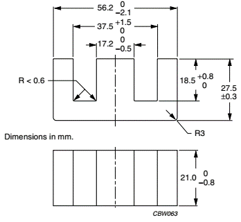
E core dimensions based on the datasheet
$$A_{p} = A_{w}.A_{c} = \lbrack b \times h\rbrack\lbrack a \times d\rbrack$$ (30)
The above equation is needed to solve for “$a$”.
To calculate the conductor’s cross sectional area in $\frac{A}{{mm}^{2}}$ ($A_{cu}$);
$$A_{cu} = \frac{I_{RMS}}{J_{RMS}}$$ (31)
Therefore;
$$A_{cu} = \frac{5,91}{5,9} = 1\frac{A}{{mm}^{2}}$$ *(32)*
Therefore the diameter of the wire in $mm$ is ($d_{wire}$);
$$d_{wire} = \sqrt{\frac{{4.A}_{cu}}{\pi}}$$ *(33)*
$$d_{wire} = \sqrt{\frac{4 \times 1}{\pi}} = 1,127mm$$ *(34)*
To find out the number of turns ($N$);
+—————————————————————–+——–+ | $$N = \frac{A_{w}{.k}{cu}}{A{cu}}$$ | (35) | | | | | Therefore | | +=================================================================+========+
$$N = \frac{186.7 \times 0.45}{1} = 84\ turns$$ (36)
full bridge Inverter design #
For the inverter, it was decided that a full bridge topology would be used to limit voltage and current stresses on the switches. Shown below is a circuit diagram of a full bridge inverter:
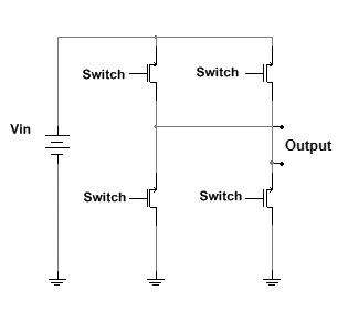
Full bridge inverter diagram
The main part of the inverter is the software needed to change the PWM signals which will discussed later on in this report. The sizing of the switches is primarily based on the currents and voltages that each switch will experience. The ratings of the switches was oversized to take into account stray inductances of the circuit which could potentially cause high voltage spikes. The switches should also be fast acting in terms of switching. The ideal input voltage of the full bridge inverter is 17Vdc.
Control #
This section will deal with the control of the buck converter and full bridge inverter. The first part will be for the buck converter.
Buck converter control #
The microcontroller used for the buck converter is the dsPIC30F4011. This particular dsPIC has six dedicated PWM channels. The input voltage of the system gets measured and processed by the dsPIC with the microcontroller’s inbuilt ADC module. Based on the ADC value measured, the corresponding duty ratio will be sent to the PWM output pin.
ADC #
The input DC voltage for the buck converter can range from 30-85Vdc, this range will be extended to 0-100Vdc. The dsPIC30F4011 can accept 5V inputs which means the input voltage needs to be scaled down to 5V. To achieve this, a voltage divider is needed and to protect the ADC pin from sinking too much current a voltage follower circuit is connected to the output of the voltage divider. Shown below is the ADC circuit;
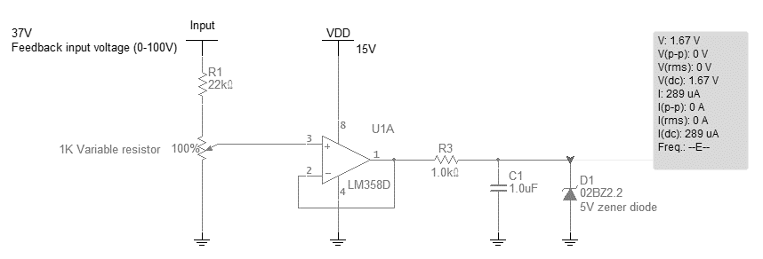
An ADC circuit with a 37V input and an output voltage of 1.67V.
Shown above is the ADC circuit used with a voltage divider using a 22kΩ (5 watt resistor) and a 1kΩ potentiometer. The output of the voltage regulator is the input of the operational amplifier (LM358) which is powered by a 15V source. Connections to the operational amplifier are wired according to the manufacturer’s datasheet6. The output of the operational amplifier is at pin 1 and is connected to a 1kΩ resistor to limit the current. The final stage is to connect a 1uF capacitor and a zener diode. Voltage stabilization is achieved with the capacitor and the zener diode (5V zener diode) offers over voltage protection for the microcontroller. The next sub section will deal with the controller for the buck converter.
Feedback control #
Small signal analysis was used on a simplified buck converter system that ignores ESR of the output capacitor, the resistance of the inductor, snubber circuits and input filter. Shown below is the buck converter that was used to derive the equations;
Buck converter diagram for small signal analysis
From the above diagram, the following AC perturbations were added along with the governing differential equations:
$$v_{Out} = V_{o} + \widetilde{v_{o}}$$
$$D = d + \widetilde{d}$$
Substituting the above perturbed variables into the differential equations yields the following Laplace transfer function ($T$) with zero initial conditions that compares the duty cycle to the output voltage.
$$T = \frac{\widetilde{v_{out}}}{\widetilde{d}} = \frac{\frac{V_{in}}{LC}}{s^{2} + s\left\lbrack \frac{1}{C.R} \right\rbrack + \left\lbrack \frac{1}{L.C} \right\rbrack}$$ *(37)*
Where $V_{out}$ output voltage; $V_{in}$ is the input voltage; $I_{L}$ the steady state inductor current; $d$ the steady state duty ratio; $R$ is the load resistance; C the output capacitor; L the inductance of the inductor
Substituting variables that will produce the maximum power transfer into the above equation:
$$T = \frac{\widetilde{v_{o}}}{\widetilde{d}} = \frac{- 1,581 \times 10^{4}s + 5,634 \times 10^{8}}{s^{2} + 5,161 \times 10^{4}s + 5,176 \times 10^{5}}$$
PID control will not be used since the D term is not needed based on the following reasons:
-
Any noise in the system will drive the system into instability since the “D” term is sensitive to erratic signal changes and noise.
-
The “D” term is usually required only for slow changing processes.
-
The “P” and “I” terms are sufficient for the control of the output voltage since all that is required is to eliminate the offset and steady state error.
Since the output voltage feedback block ${(T}_{FB})$ has been determined, it can be incorporated in the control system diagram with the transfer function “$T”$ to give the figure below.
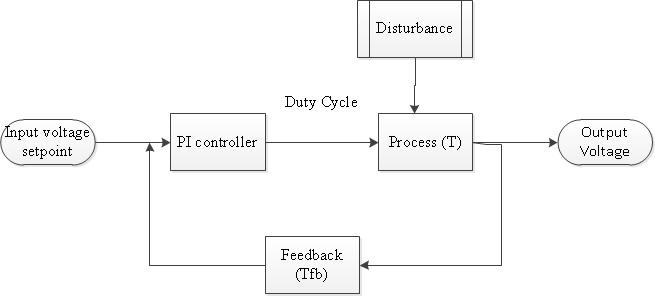
Control system flow diagram
The PI controller will be done programmed in software. Shown below is a equation of the PI controller:
$$C(t) = k_{p}.e(t) + k_{i}.\int_{}^{}{e(t).dt}$$ *(38)*
Where $C(t)$ and $e(t)$ are the “PI controller” and “error” function. $k_{p}$ and $k_{i}$ are the “proportional” and “integral” constants (values between 0.00001 and 10).
Shown below is the flow diagram of the code that will generate the correct duty cycle for the MOSFET. It is crucial to tune the integral and proportional gains correctly and will be implemented by software code.
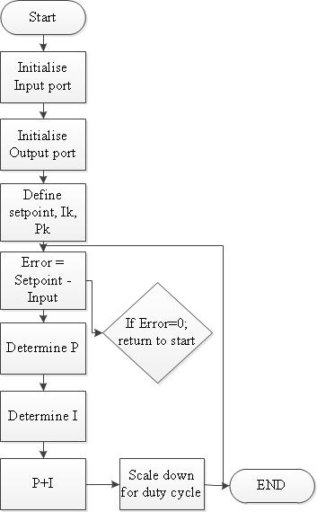
Program flow diagram for PI control
The code was developed by using MPLAB IDE X7 with C30 compiler and Flowcode. Shown below is a flow diagram of Flowcode. Initial step was to set the oscillator and clock speed, then to set up the ADC and PWM modules. The final step was to link the ADC measurements with the PWM module. The $k_{p}$ and $k_{i}$terms of the PI controller were tuned until the right response was reached. Shown below is the flow diagram of the software in flowcode:
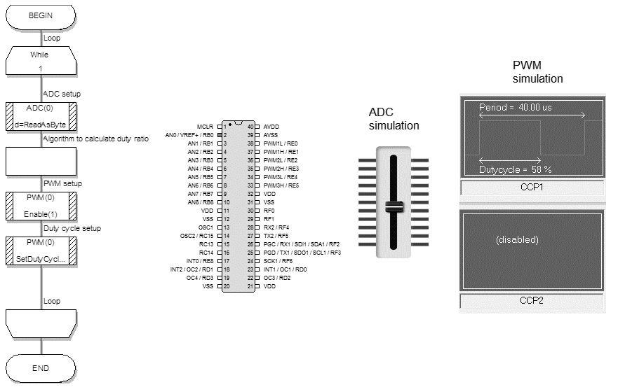
Software implementation in Flowcode8
Full bridge inverter control #
The full bridge inverter’s switching scheme is more complicated than the buck converter’s scheme since a pure sine wave has to be generated. The microcontroller needs to have a minimum of 2 PWM channels since only 2 channels are needed. Only two switches will be subjected to changing duty ratios while the other 2 will be either set high or low at 50Hz intervals.
The switches will switch based on a sinewave. The sinewave will be divided into a specific amount of discrete points, the more the points the higher the accuracy of the sinewave. The software code implemented a 256 point sinewave table.
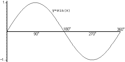
Sinewave function used to generate discrete points
Shown below is a circuit diagram of the switches that will be programmed to switch at different duty ratios.
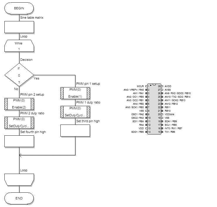
Inverter software flowchart in Flowcode
Unlike the buck PWM control which was simulated in Flowcode, the inverter code was tested on Proteus since the code required variable duty ratio changes.
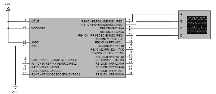
Inverter PWM pins simulation in setup Proteus9
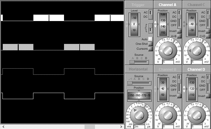
Duty cycle output measurements on all 4 pins
Full inverter system simulation setup in Proteus
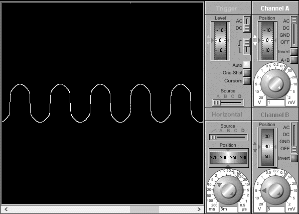
Sinewave output of inverter circuit
Gate drive design and MOSFEt selection #
The project requires 5 MOSFET switches and each MOSFET requires a minimum of 10V to be switched “ON” and the microcontrollers at most can only generate 5V PWM signals (or 3,3V for some dsPICs) which is not adequate.
Designing and choosing the right MOSFET driver for the step down converter and inverter requires a thorough understanding of power dissipation in relation to the MOSFET's gate charge and operating frequencies, which in this case was chosen to be in the 20-25kHz. The equivalent capacitance value of the MOSFET needs to be adequately charged in order for the switching to be smooth and timely. The MOSFETs selected for both the buck converter and the inverter were the 2SK996 which has a 600V 10A rating10. Selection criteria of the MOSFETs was based on the possible spikes the converters
Shown below is a diagram of typical power MOSFET and the associated capacitances.
height=“1.8583333333333334in”}

Power MOSFET diagram
height=“2.475in”}

MOSFET switching behavior11
The threshold voltage ($V_{GS(th)})$is the minimum gate voltage that initiates drain current flow.
The charging and discharging the gate of a MOSFET requires the same amount of energy, regardless of how fast or slow the rise and fall of the gate voltage occurs. Therefore, the current drive capability of the MOSFET driver does not affect the power dissipation in the driver due to the capacitive load of the MOSFET gate.
There are three aspects of power dissipation in a MOSFET driver12:
-
The charging and discharging of the gate capacitance of the MOSFET.
-
Quiescent current drawn of the MOSFET driver.
-
Power dissipation due to cross-conduction (shoot-through) current in the MOSFET driver.
There are numerous gate driver modules in the market. Initially the “IR2110 dual high side and low side” MOSFET driver was experimented with to power the MOSFETs of the inverter but problems arose since the output signals were distorted. Another option was to try a MCPL isolated gate driver module since it was readily available but it too caused problems since it was sensitive to the resistors and capacitors and the grounding of the input signals as based on its datasheet. The next step was to try a “HCPL 3120 IGBT optocoupler” which worked as specified with a few components. Shown below is a circuit diagram as based on the datasheet:
![[]{#_Ref400815565 .anchor}Figure 36.](/focus/projects/inverter-design-from-first-principles/media/image27.png)
Above ciruit diagram from the HCPL 3120 datasheet
Looking at the demarcated area in Figure 36 with conjunction to the HCPL 3120 datasheet13, pin 2 is connected to the microcontroller’s PWM output with a 1kΩ resistor and pin 4 is connected to the same ground as the microcontroller. Pin 8 is connected to the 15V source of the power supply and pin 5 is connected with the 15V power supply’s ground. The output pins 7 and 8 are bridged and connected to the $R_{g}$ resistor whose value is calculated by using the following formula as based from the datasheet:
$$R_{g} \geq \ \frac{V_{cc} - V_{EE} - V_{OL}}{I_{OLPEAK}}$$ (39)
Where $R_{g}$ is the gate resistance (Ohms, Ω); $V_{EE}$is the ground potential and $V_{CC}$ is the supply source magnitude (Volts, V); $V_{OL}$ is selected to be 2V and $I_{OLPEAK}$ to be 2,5A.
Putting values in the above equation yields:
$$R_{g} \geq \ \frac{15 - 2}{2,5} \geq 5,2\mathrm{\Omega}$$ (40)
$R_{g}$ was selected to be 1kΩ to satisfy the above equation.
Output LC filter design #
Theoretically the output of the inverter stage is a 12Vac 50Hz signal which is composed of a train of pulses. To convert these pulses into a smooth sine wave, a low pass filter needs to be designed.
First the output of the inverter needs to be boosted up to 230Vac with the use of a transformer. The transformer chosen has a rating of 160VA with double input and output options. The toroidal transformer was wired in parallel at the input section (two 12V input wires) and in series at the output section (two 115V output wires). The low pass LC filter was based on the following equation:
$$f_{cutoff} = \frac{1}{2\pi\sqrt{L_{f}.C_{f}}}$$ *(41)*
Where $f_{cutoff}$ is the cutoff frequency (Hertz, Hz) which was set to be about 5% of the switching frequency (5% of 25kHz = 1250Hz ); $L_{f}$ is the inductance of the filter inductor (Henry, H) and $C_{f}$ is the capacitance of the filter capacitor (Farad, F).
Since the switching frequency of the inverter circuit is many orders higher than the fundamental frequency, a higher frequency can be set to small components can be used to create the filter. The large distance between the unwanted harmonics and the fundamental frequency is also beneficial because it allows for a large margin of error in the filter values.
The component values used was based on availability while bearing in mind that the transformer itself also has inductance. The final values of the components and the output filter of the circuit is shown below:
Diagram of the LC filter circuit
Shown below is a gain response bode plot of the LC filter:
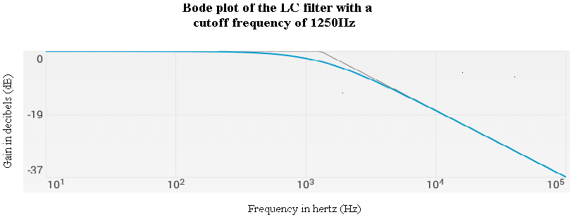
Bode plot of the LC filter with a cutoff frequency of 1250Hz
Auxiliary Power Circuit #
The auxiliary power circuit is powered by the mains supply which is 230Vac at 50Hz. The components that require power is the dspic33, the dspic30, a 12V fan and the three gate drive chips. Ideally a single 230V/12V step down transformer with a high current rating (2A output) would be sufficient to power all the components. However, a 1A 230V/12V transformer and a 1A 230V/6V was used since they were readily available.
The 6V transformer was used to power the two microcontrollers and the 15V to power the gate drive chips and the fan. Full bridge rectifiers with suitable capacitors were connected to each transformer to provide DC outputs. Voltage regulators were used to supply a steady DC voltage for the components. A 3.3V14 and 5V15 voltage regulator was used to power the dsPIC33 and dsPIC30 microcontrollers respectively. A 15V voltage regulator16 was used to power the MOSFET drivers for the buck converter and inverter. Five 15V voltage regulators were used to power each of the gate drivers since isolation was needed. Two transformers with double 12V outputs were used to power the inverter circuits. Two capacitors are connected to each of the mentioned voltage regulators as specified by their respective datasheets. Shown below is the circuit and simulation of the auxiliary power circuit and its output voltages (only one of the five 15V voltage was simulated to save space):
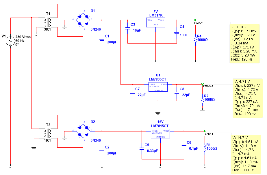
Diagram of the auxiliary power circuit and its output voltages
Thermal design #
Heat sinks are used for cooling of power semiconductor devices. The junction temperature of power devices had to be kept within reasonable bounds. A heat conduction path had to be created between the case of the device and the ambient air so that the thermal resistance between the case and the ambient is minimized. The choice of heat sinks depends on the allowable junction temperature the device can tolerate.
Buck converter switch #
The total switching losses ($P_{buck,\ switch}$) are given by the calculation below for the buck converter switch:
$$P_{buck,\ switch} = \frac{1}{2}\left( t_{r} - t_{f} \right)V_{ds}.I_{o}.F_{sw} + V_{CE}.I_{D}$$ (42)
Where $t_{r}$ and $t_{f}$ is the rise and fall time respectively of the switch (s, seconds); $V_{ds}$ is the drain-source voltage of the switch (V, volts), $I_{o}$ is the current the MOSFET is conducting during the switching transition (A, amperes); $F_{sw}$ is the switching frequency (Hz, hertz); $V_{CE}$ the voltage of the switch when it is conducting current (A, amperes) and $I_{D}$ is the drain current (A, amperes).
Based on the above equation;
$$P_{buck,\ switch} = \frac{1}{2}\left( 27 \times 10^{- 9} - 15 \times 10^{- 9} \right) \times 17 \times 5.88 \times 25 \times 10^{3} + 1.7 \times 5.88 = 11.49W$$ (43)
The calculated dissipated power will be used in the equation below to calculate the thermal resistance ($R_{\theta JA}$) of the heatsink.
$$R_{\theta JA} = \frac{T_{junction} - T_{ambient}}{P_{buck,\ switch}}$$ (44)
Where $R_{\theta JA}$ is the thermal resistance of the heatsink (°C/W, Celcius per Watt, );$\ T_{junction}$ and$\ T_{ambient}$ is the temperature of the MOSFET junction and the ambient air (°C, Celcius) and $P_{buck,\ switch}$ is the calculated dissipated power (W, watts).
$$R_{\theta JA} = \frac{150 - 50}{11.49} = 8.70{^\circ}C/W$$ (45)
A suitable heatsink was used based on the above calculated value.
Full bridge inverter switches #
A similar process was followed to design for the heatsinks needed for each inverter MOSFET. Since the duty cycle is constantly changing, approximations were made to simplify the calculation.
$$P_{inverter,\ switch} = \frac{1}{2}\left( t_{r} - t_{f} \right)V_{ds}.I_{o}.F_{sw} + V_{CE}.I_{D}$$ *(46)*
$$P_{inverter,\ switch} = \frac{1}{2}\left( 27 \times 10^{- 9} - 15 \times 10^{- 9} \right) \times 17 \times 2.94 \times 25 \times 10^{3} + 1.7 \times 2.94 = 6.67W$$ *(47)*
The calculated dissipated power will be used in the equation below to calculate the thermal resistance ($R_{\theta JA}$) of the heatsink.
$$R_{\theta JA} = \frac{T_{junction} - T_{ambient}}{P_{buck,\ switch}}$$ *(48)*
$$R_{\theta JA} = \frac{150 - 50}{6.67} = 14.99{^\circ}C/W$$ *(49)*
A suitable heatsink was used based on the above calculated value.
Snubber design #
Snubber circuits are used to protect MOSFETs and reduce EMI. There are two types of snubber circuits, dissipative and non-dissipative snubber circuits. Dissipative snubber circuits employ a capacitor, resistor and a diode to absorb voltage and current spikes. Non dissipative snubbers replace the resistor with an inductor which acts like an energy storage device rather than a dissipative component.
The inductor’s leakage inductance induces high transients in the switch, which requires selecting a switching device with an excessive voltage rating. A passive voltage clamp is needed to suppress the voltage overshoot during the turn-off transition of the MOSFET. This circuit limits the peak switch voltage and thus reducing the power dissipation in the switching device. The total dissipated energy remains the same, but it is now divided between the clamp resistor and the MOSFET.
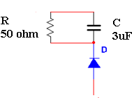
Snubber circuit for buck converter switch
Based on the above circuit, the parasitic inductance of the inductor is discharged into the capacitor during each switching cycle. The next step is to determine the value of the capacitor. The value of the capacitor is selected based upon the amount of energy that this leakage inductance stores plus the initial energy stored in the capacitor from the input voltage and the reflected output voltage. The equation below determines the minimum capacitor value;
$$C_{snubber} = \frac{{2.L}_{l}.{I_{peak}}^{2}}{{V_{out}}^{2}}$$ *(50)*
Where $C_{snubber}$ is the snubber capacitor (C, Farads); $L_{l}$ is the leakage inductance of the inductor (H, Henry) and is assumed to be 6% of the inductance; $I_{peak}$is the peak value of the primary current at the turn off time of the MOSFET (A, Amperes);and $V_{out}$ is the output voltage (V, Volts).
Inserting the variable values in the above equation with the assumption that the leakage inductance ($L_{l}$) is 6% of the primary inductance (non-ideal inductor since it was wound by hand), the primary snubber ($C_{pri,snub}$) was found to be:
$$C_{snubber} = \frac{2 \times (0.06 \times 830 \times 10^{- 6}) \times 7.35}{17^{2}} = 2.53uF \approx 3uF$$ *(51)*
The snubber resistor is selected such that the RC time constant is much longer than the switching period. This resistor must not only dissipate the energy stored in the leakage inductance, but also the voltage due to the DC bias of the capacitor. The power dissipated by this snubber circuit is calculated by using the following equation:
$$P_{\ snubber} = {0,833.L}_{l}.{I_{peak}}^{2}.f_{sw}$$ *(52)*
$$P_{\ snubber} = 0,833 \times 0.06 \times 830 \times 10^{- 6} \times {7.35}^{2} \times 25 \times 10^{3} = 5.6W$$
Based on the above power dissipation, the resistor value can be calculated by using the following equation:
$$R_{snubber} = \frac{{V_{out}}^{2}}{P_{snubber}}$$ *(53)*
$$R_{snubber} = \frac{17^{2}}{5.6} = 51.60\Omega \approx 50\Omega$$ (54)
The diode needed has to have a voltage rating dictated by the equation below:
+————————————-+———————————————————————+——–+ | | $$V_{diode,\ snubber} = V_{in,max} + (SF \times V_{out})$$ | (55) | +=====================================+=====================================+===============================+=======:+ | | | | +————————————-+————————————-+——————————-+——–+ | $$V_{diode,\ snubber} = 100 + (2,5 \times 17) = 142.50V \approx 150V$$ | (56) | +—————————————————————————+—————————————-+
The SF is a safety factor co-efficient to take into account transient oscillations of the voltage and current.
Efficiency #
The efficiency of the converter was worked out by finding out the losses of the following subsystems [11]:
Input filter #
The input filter’s main power dissipation is contributed by the bridge rectifier.
$$P_{bridge} = {2.V}_{cond,b}.I_{cond,b}$$ *(57)*
Where $V_{cond,b}$ is the bridge rectifier diodes’ voltage when conducting (0,7V according to the datasheet) and $I_{cond,b}$ is the current going through the bridge rectifier diodes while conducting.
Substituting the variables with the values in equation
$$P_{bridge} = 2 \times 0,7 \times 5.88 = 8.232W$$
MOSFET and gate drive #
The gate driver datasheet refers to a power dissipation 0.295W17 (translates to about 1.2W for five gate drivers).
The MOSFET exhibits two power losses, conduction loss and switching loss. The losses have already been calculated as approximately 12W for the buck converter’s switch and 7W for each of the inverter switches.
Auxiliary power circuit #
The power consumed by the additional power sources are mainly related to the voltage regulators used is approximately 5W for each regulator.
Microcontroller and feedback network #
The microcontroller dissipates energy in the range of nano watts which can be considered negligible. The operational amplifier used for the voltage feedback circuit dissipates 200mW18.
Snubbers #
The power dissipation of the combined snubber circuits has been calculated to be 5.6W.
Total efficiency #
Adding up all the power losses ($P_{loss}$) .
$$Effciency = \ \frac{P_{out}}{P_{in}}$$ *(58)*
$$Where\ P_{in} = V_{in}I_{in} = P_{out} + P_{loss}$$
$$P_{out} = V_{out}I_{out}$$
$$Effciency = \ \frac{100}{\begin{array}{r} 100 + 78.8 \end{array}} = 55.93%$$
Even though this efficiency value seems close to the 60%, there are other losses that are not accounted for like:
-
Parasitic losses
-
Leakage inductances
-
ESR resistances of the capacitors
The expected efficiency therefore could be between 40% to 50%.
Safety #
The buck converter by its input side has a current sensitive fuse that will trip if a current exceeding 6A is detected.
Another safety feature was the connection of the earth wire to the metallic casing of the system.
The housing of the overall system is insulated from the user.
CONCLUSION #
SUMMARY OF THE WORK #
The following has been achieved:
-
Derivation of the buck converter’s governing equations from first principles.
-
Derivation of the buck converter’s output voltage to duty ratio transfer function.
-
Design of a inductor and wound it by hand.
-
Created code for the dsPIC30F to sense voltage as an input and generate a PWM signal as an output.
-
Created software for the dsPIC30F to sense voltage as an input and generate a PWM signal as an output.
-
Created software for the dsPIC33F to generate a sinewave for the full bridge inverter.
-
Calculations for most of the losses in the system to determine the theoretical efficiency.
-
Simulation of the buck converter with PSpice.
-
Simulation of the full bridge inverter with hardware and software with Proteus.
-
Design of the snubber circuit.
-
Thermal design
-
Building of all the sub circuits with the use of veraboards and PCB.
-
Inverter testing and full system integration
SUMMARY OF THE OBSERVATIONS AND FINDINGS #
A significant amount of this project has been spent on the following:
-
Trying to implement the code with assembler language rather than C.
-
Winding the inductor by hand.
-
Trying to sort out compilers to make the software communicate with the physical dsPIC.
-
Gate drive circuit design.
SUGGESTIONS FOR FUTURE WORK #
The following is suggested for future work:
-
Implementing soft switching within the converter to minimize switching losses and thus improve efficiency.
-
Replacing the output diode of the buck converter with a MOSFET, to increase the system’s overall efficiency.
-
Selecting a different DC-DC converter topology to meet specifications.
-
Implementing a double loop system to yield better converter dynamics.
References #
[1] T. Ayodele, A. Jimoh, J. Munda and J. Agee, “Challenges of Grid Integration of Wind Power on Power System Grid Integrity: A Review,” International Journal of Renewable Energy Research, 2012.
[2] Department of Energy: Republic of South Africa, “Grid integration of wind turbines:What happens when the wind stops blowing?,” 2012.
[3] M. N. M. M. D. Ali Keyhani, Integration of green and Renewable Energy in Electric Power Systems, New Jersey: John Wiley & Sons, 2010.
[4] RSA Wind Turbines Connection Conditions, Grid Code Requirements for Wind Turbines Connected to Distribution or Transmission Systems in South Africa, Germinston.
[5] S. Heier, Grid Integration of Wind Energy Conversion Systems, West Sussex: John Wiley & Sons Ltd, 2007.
[6] DEWI; E.ON Netz; EWI; RWE Transport Grid, Electricity; VE Transmission, “Planning of the Grid Integration of Wind Energy in Germany Onshore and Offshore up to the Year 2020,” Cologne, 2005.
[7] International Electrotechnical Commision, “Grid Integration of Large-Capacity Renewable Energy Sources and use of large-capacity Electrical Energy Storage,” Switzerpajd, 2012.
[8] “Introduction to Switched- Mode Power Supply (SMPS) Circuits,” EE IIT, Kharagpu.
[9] Incorporated Microchip Technology, “Introduction to SMPS control techniques,” pp. 1-29, 2006.
[10] Mohan, Undeland and Robbins, Power Electronics: Converters, Applications and Design, John Wiley & Sons, 2003.
[11] R. Fassler, “Energy Efficiency Standards for Power Supplies,” San Jose, USA, 2009.
[12] V. C. V. Alex Van der Bassche, “Inductors and transformers,” 2000, p. Appendix A.
[13] K.-S. L. Ecya B Joffe, “Grounds for grounding - A circuit-to-system handbook,” pp. 225-233.
[14] M. Majeika, “EMC Specifications and PCB Guidelines for SMPS Devices,” ON Semiconductor, 2009.
[15] B. Choi and B. Cho, “Intermediate line filter design to meet both impedance compatibility and EMI specifications,” Power Electronics, IEEE Transactions, vol. 10, no. 5, pp. 583-588, 1995.
[16] W. McMurray, “Optimum Snubbers for Power Semiconductors,” IEEE Transactions, Vols. IA-8, pp. 593-600, Sept. 1972.
[17] L. Hsiu, M. Goldman, R. Carlsten, A. Witulski and W. Kerwin, “Characterization and Comparison of Noise Generation for Quasi-Resonant and Pulsewidth-Modulated Converters,” IEEE Transactions on Power Electronics, vol. Volume 9, no. No. 4, July 1994.
[18] A. Guerra and F. Vallone, “Stage, Efficiency in SMPS Output,” International Rectifier, El Segundo CA, 1998.
[19] L. E.Jones, Strategies and Decision Support Systems for Integrating Variable Energy Resources in Control Centers for Relibale Grid Operations, Washington.
[20] University of Massachusetts, “Wind Power: Performance & Economics,” Amherst.
[21] D. Justus, “Case Study 5: Wind Power Integration into Electricity Systems,” International Energy Technology Collaboration and Climate Change Mitigation, 2005.
[22] National Conference of State Legislatures; National Wind Coordinating Collaborative, “Integrating Wind Power Into the Electric Grid: Perspectives for Policymakers,” Denver, 2009.
[23] K. Hagemann, “South Africa's Wind Power Potential,” SANEA, Cape Town, 2013. #
-
Rds is the drain source resistance. ↩︎
-
“RS602 Single Phase Bridge Rectifier” by Rectron Semiconductor. ↩︎
-
“30EPF Fast soft recovery rectifier diode” datasheet by International Rectifier ↩︎
-
“SIFERRIT material N27” datasheet by TDK ↩︎
-
“E55/28/21 E cores and accessories” by Ferroxcube ↩︎
-
“LM358 Low Power Dual Operational Amplifiers” datasheet by Texas Instruments ↩︎
-
“MPLAB X IDE” is a free, integrated toolset for the development of embedded applications on Microchip's PIC and dsPIC microcontrollers ↩︎
-
“Flowcode” is a development environment produced by Matrix Multimedia for programming embedded devices such as PIC, AVR (including Arduino) and ARM using flowcharts instead of a textual programming language. ↩︎
-
“Proteus” is a software application for simulating microcontroller based circuits and creating printed circuit-board layouts. ↩︎
-
“TOSHIBA Field Effect Transistor Silicon N Channel MOS Type (π−MOSV) 2SK996” by Toshiba. ↩︎
-
Figure 29 and Figure 30 are from an application note (558) written by Ralph Locher. “Introduction to Power MOSFETs and their Applications” by Fairchild Semiconductors. ↩︎
-
The equations are from an application note (AN799) written by Jamie Dunn. “Matching MOSFET Drivers to MOSFETs” by Microchip Technology Inc. ↩︎
-
“HCPL 3120 – 2.0 Amp Output Current IGBT Gate Drive Optocoupler” by Hewlett Packard. ↩︎
-
“LM1117-N/LM1117I 800mA Low-Dropout Linear Regulator” datasheet by Texas Instruments. ↩︎
-
“L7805C 5V regulator” datasheet by ST. ↩︎
-
“L7815C 15V regulator” datasheet by ST. ↩︎
-
“HCPL 3120 – 2.0 Amp Output Current IGBT Gate Drive Optocoupler” by Hewlett Packard. ↩︎
-
“LM158 Low Power Dual Operational Amplifiers” datasheet by Texas Instruments. ↩︎